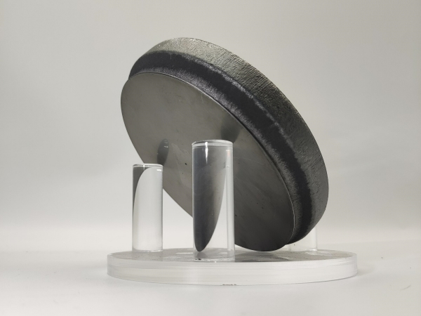
— Technological Evolution from Conventional Grinding to Atomic-Scale Manufacturing
With the rapid development of new energy vehicles, photovoltaic energy storage, AI servers, and 5G communications, the third-generation semiconductor material—silicon carbide (SiC)—is increasingly becoming a core substrate for high-end power electronics. Compared with traditional silicon (Si), SiC offers a wider bandgap, higher breakdown electric field, superior thermal conductivity, and excellent high-temperature stability. These properties enable significantly lower conduction losses, higher energy conversion efficiency, and electronic systems with higher power density and operating temperature.
At present, SiC devices are widely used in key applications such as traction inverters for electric vehicles, high-voltage power transmission systems, rail transportation, industrial frequency converters, and aerospace power supplies. However, the very physical advantages of SiC also make it one of the most difficult semiconductor materials to process. With a Mohs hardness of approximately 9.5—second only to diamond—SiC also exhibits pronounced brittleness and strong chemical inertness. During processing, SiC wafers are highly susceptible to cracking, edge chipping, scratching, and deep subsurface damage. These defects degrade device reliability, shorten service life, and significantly increase subsequent polishing costs.
Therefore, achieving high-efficiency, low-damage, and nanometer- or even atomic-level precision machining of SiC wafers has become a major research focus in advanced manufacturing worldwide.
1. Conventional SiC Wafer Processing and Grinding-Induced Damage
Current SiC wafer manufacturing typically involves multiple steps, including slicing, double-side grinding, single-side fine grinding, chemical mechanical polishing (CMP), thinning, and final polishing. Among these, grinding and polishing are the most critical processes determining final wafer quality.
In conventional processing, double-side grinding is primarily used for rapid wafer planarization and thickness uniformity improvement. Its main objectives include reducing total thickness variation (TTV), improving parallelism, and removing subsurface damage induced by slicing.
Due to the extremely high hardness of SiC, randomly distributed diamond abrasives during double-side grinding generate severe impact on the surface, leading to deep scratches, median cracks, transverse cracks, and significant subsurface damage. Studies show that after conventional double-side grinding, the surface roughness of SiC wafers typically remains above 0.1 μm, far from the nanometer-level requirements of semiconductor device fabrication.
2. Process Optimization: Structured Grinding and Ultrasonic Assistance
To address these issues, researchers have proposed optimized grinding structures and processing methods. One example is the honeycomb-structured grinding pad, in which diamond abrasives are embedded within hard honeycomb cavities and semi-fixed using a soft gel binder. This design promotes more uniform abrasive distribution, reduces local stress concentration, suppresses crack propagation, and improves surface quality.
Experimental results show that this structure can reduce surface roughness to 75–125 nm, significantly outperforming conventional grinding methods.
 Figure 1: Grinding operation using a rigid honeycomb-structured grinding wheel.
3. Ultrasonic-Assisted Grinding: Higher Efficiency vs. Surface Damage
To further improve material removal rate (MRR), ultrasonic-assisted grinding has been introduced. By applying high-frequency ultrasonic vibrations during grinding, abrasives undergo periodic impact and intermittent contact, reducing average cutting forces and improving chip evacuation.
Ultrasonic vibration also enhances localized brittle fracture, making SiC easier to remove and thus significantly increasing MRR. However, experiments also show that ultrasonic impact exacerbates crack propagation and surface fragmentation, leading to degraded surface roughness.
This reveals a fundamental contradiction in SiC machining:
high efficiency versus low damage. Balancing MRR improvement and subsurface damage control remains a key challenge in grinding processes.
4. Chemical Mechanical Polishing (CMP): The Core of Near-Defect-Free Finishing
Because grinding still leaves a relatively deep damaged layer, chemical mechanical polishing (CMP) is required for near-defect-free finishing. CMP is currently the most mature industrial SiC finishing technology. Its mechanism is not purely mechanical removal but a combination of
chemical softening and mechanical abrasion.
Specifically, an oxidizing agent first forms a soft oxide layer on the SiC surface, which is then gradually removed by nanoscale abrasives. Since the oxide layer is much softer than SiC, mechanical damage is significantly reduced.
Abrasive size strongly influences CMP performance: larger SiO₂ particles increase MRR but introduce more scratches and defects, while smaller particles produce smoother surfaces but lower efficiency. Thus, CMP is essentially a trade-off between processing rate and surface quality.
5. Catalysis-Enhanced CMP: Toward Atomic-Level Surfaces
In recent years, catalyst-assisted CMP has become a major research focus. By introducing catalytic nanoparticles into the slurry, the decomposition of H₂O₂ is promoted, generating highly reactive OH radicals. These radicals strongly oxidize the SiC surface, significantly accelerating material removal.
Experimental results show that catalyst-assisted CMP can produce distinct atomic step structures on SiC surfaces and achieve ultra-smooth surfaces with Ra ≈ 0.05 nm, approaching the theoretical limit.
 Figure 2: Surface measurement results of 4H-SiC wafers processed by catalyst nanoparticle-assisted CMP.
6. Emerging Energy-Field Assisted Polishing Technologies
Despite CMP’s excellent surface quality, its main drawback is low MRR. As a result, several new energy-field-assisted polishing technologies have emerged, including:
Electrochemical mechanical polishing (ECMP)
Laser-assisted polishing (LAP)
Ultraviolet-assisted polishing (UAP)
6.1 Electrochemical Mechanical Polishing (ECMP)
ECMP uses an external electric field to induce anodic oxidation on the SiC surface, reducing mechanical removal difficulty and damage. Compared with CMP, ECMP offers higher efficiency, reduced slurry consumption, and better environmental performance.
Studies show that ECMP can achieve surface roughness of Sq = 1–2 nm and increase MRR up to 23 μm/h.
 Figure 3: Schematic diagram of slurry-free ECMP.
6.2 Laser-Assisted Polishing (LAP)
LAP uses a CO₂ laser to locally heat the SiC surface, inducing thermal oxidation and localized softening, while also generating microcracks that reduce material hardness and improve subsequent removal efficiency.
Research indicates that LAP can increase MRR by approximately 79% compared with conventional mechanical polishing, highlighting laser-induced surface modification as a promising direction.
 Figure 4: Principle diagram of the LAP process.
6.3 Ultraviolet-Assisted Polishing (UAP)
UAP utilizes ultraviolet light to activate photocatalysts such as TiO₂, generating electron–hole pairs that further produce OH radicals, accelerating surface oxidation.
While UAP can further improve MRR and surface quality compared to CMP, it still faces challenges including process stability, high equipment cost, and difficulties in industrial-scale implementation.
 Figure 5: Principle of UAP processing.
7. Ultra-Precision Grinding: A Future Direction for SiC Manufacturing
Compared with conventional grinding and polishing, ultra-precision grinding is emerging as a key future direction for SiC machining. It uses a rotational processing mechanism with advantages such as:
- Uniform abrasive distribution
- Lower grinding forces
- High automation level
- Suitability for large-diameter wafers
Compared with traditional grinding, it significantly reduces subsurface damage depth and shortens subsequent CMP time, making it highly promising for large-scale SiC wafer production.
Currently, Japanese companies lead in this field. For example:
DISCO’s DFG8830 adopts a “three-rough, one-fine” multi-spindle structure and supports
6-inch SiC wafer processing.
ACCRETECH’s HRG series uses high-rigidity spindles and low-vibration design, achieving TTV < 3 μm and wafer thickness variation within ±3 μm.
 Figure 6: Ultra-precision grinding using a rotating workpiece configuration.
 Figure 7: DISCO DFG8830 SiC wafer grinding machine (disc type).
 Figure 8: ACCRETECH SiC wafer grinders: (a) HRG200X, (b) HRG300.
In recent years, domestic manufacturers have also accelerated development in this field, including machines such as TFG-3200, CMG200, and MX-SSG. These systems already support 8-inch SiC wafer processing, marking significant progress in localization of high-end equipment.
 Figure 9: Domestic ultra-precision SiC wafer grinding machine.
8. Subsurface Damage: The Core Challenge in SiC Machining
Regardless of grinding method, subsurface damage remains the most critical challenge in SiC processing. Although diamond wheels provide high efficiency, they inevitably introduce microcracks, residual stress, and lattice distortion.
The most severe issue is invisible subsurface cracking, which increases CMP time and significantly reduces wafer yield and device lifetime.
Studies show that as grinding depth decreases, chipping and cracking are reduced, and the material removal mechanism gradually transitions from brittle fracture to ductile deformation. This indicates that SiC can potentially be processed in the ductile regime if cutting depth is precisely controlled.
 Figure 10: Surface/subsurface characteristics of 6H-SiC wafers under different grinding conditions.
9. Theoretical Modeling and Process Prediction
To achieve precise process control, researchers have developed numerous theoretical models, including abrasive penetration depth models, surface roughness prediction models, and subsurface damage models.
The undeformed chip thickness is widely regarded as a key parameter governing crack formation and material removal mode. Based on stochastic abrasive distribution models, nano-indentation theory, and Rayleigh distribution models, researchers have predicted surface roughness and subsurface damage.
Some models already achieve prediction errors below 6%, but a complete theoretical framework for rotational ultra-precision grinding of SiC is still lacking.
 Figure 11: Comparison between predicted and measured surface roughness under different grinding parameters.
  Figure 12: Median/radial crack models for brittle materials based on indentation theory.
10. Conclusion: Toward Atomic-Level SiC Manufacturing
Overall, ultra-precision machining of SiC wafers can be understood as a long-term “battle against cracks and damage.” From conventional grinding to CMP, from energy-field-assisted polishing to ultra-precision grinding, manufacturing technology is continuously approaching the theoretical limits of SiC processing.
In the future, with advances in high-end equipment, AI-driven process optimization, in-situ metrology, and atomic-scale simulation, SiC wafer fabrication is expected to achieve high efficiency, low damage, low cost, and atomic-level precision.
This will become a fundamental competitive frontier for the next generation of power semiconductor industry.

With the continuous advancement of ultra-precision machining technologies, SiC wafers are gradually overcoming the “hard and brittle” processing bottleneck. From conventional grinding to atomic-scale manufacturing, process innovations are driving the wider adoption of silicon carbide in EVs, power electronics, and high-frequency devices.
JXT supplies 2–8 inch silicon carbide (SiC) substrates for both research and industrial applications.