JXT has more than 10 years of experience in semiconductor wafer slicing, chamfering, grinding, polishing, laser processing, vapor phase epitaxy, thin film deposition, and laser engraving,etching, oxidation process, sputtering coating and other services.JXT’s products are in line with international production standards and have passed environmental quality certification, including ISO9001 and ISO4001 certification, as well as international RoHS and REACH certification.JXT keeps paying attention to each process of the products like the crystal quality, production and processing, inspection and packaging, we try our best to improve the product quality and our services.
The Manufacturing Process Flow Chart of JXT’s wafers
Crystal Raw
Bar Rolling
Cutting
Annealing
Chamfering
Grinding
Delivery
Packaging
Cleaning
Laser
Testing
Polishing
The Processing Technology for JXT's Substrate Wafers
Laser
Etched
Patterning
Oxidation
Bonding
Epitaxy
Sputtering
Coating
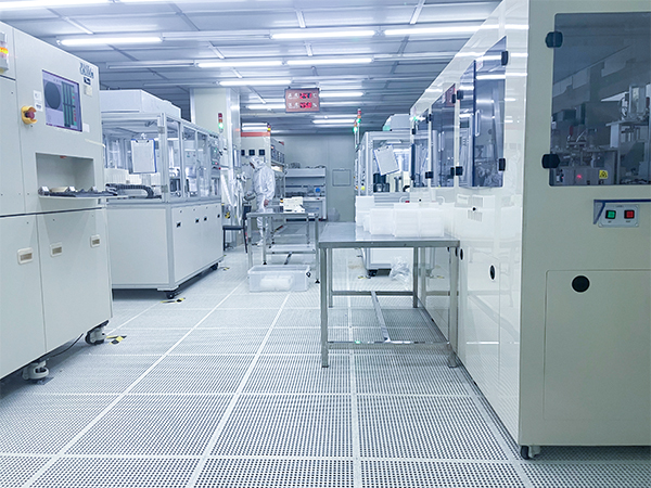
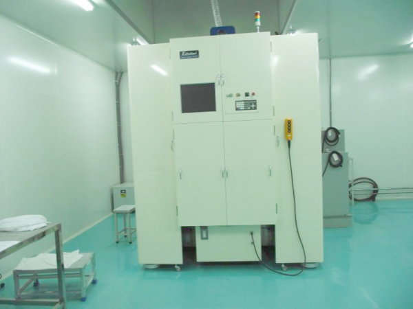
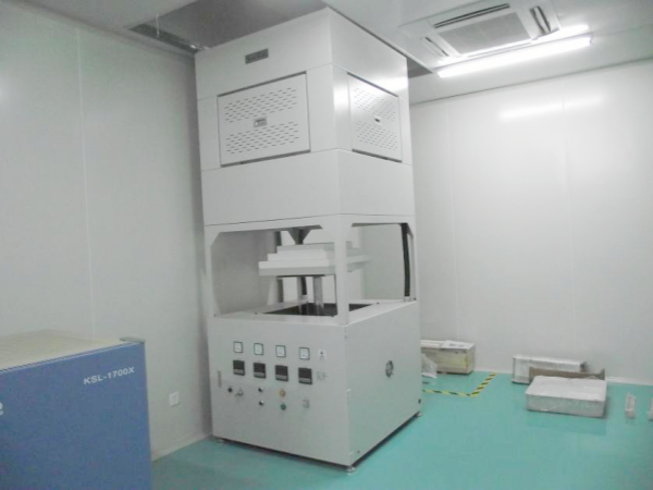
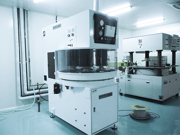
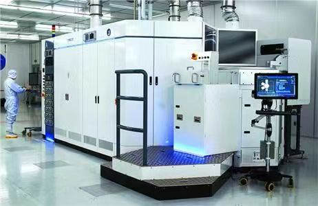
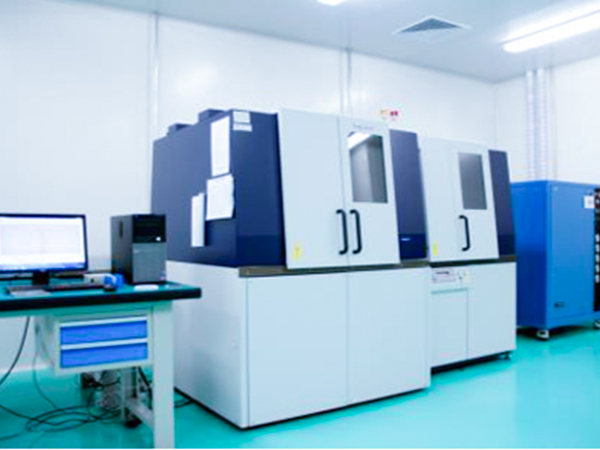
Production Equipments
-
Dust-free environment
-
Wafer Multi-line Cutting Machine
-
Wafer Annealing Furnace
-
Chamfering Machine
-
CMP Polishing Machine
-
Laser Machine
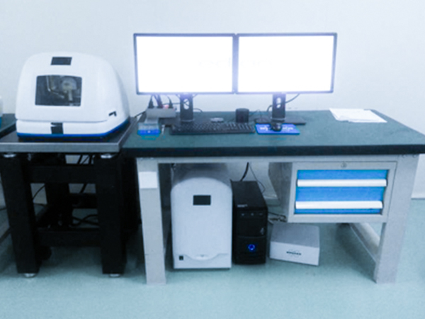
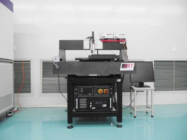
Testing Equipments
-
Testing equipment
-
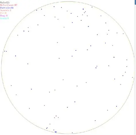
Particle Scratch Tester
-
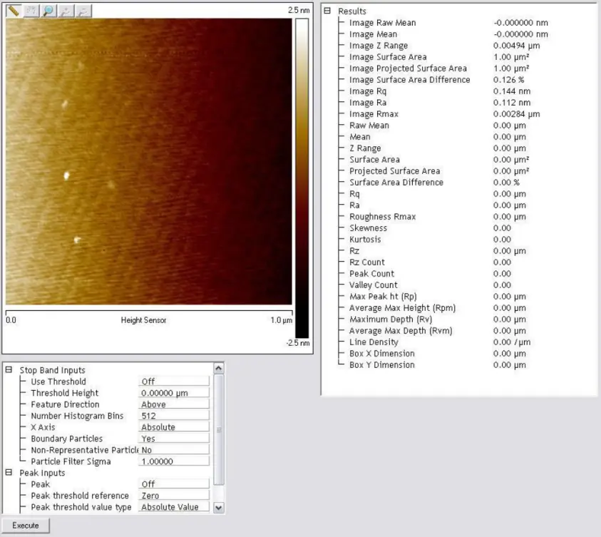
Roughness Tester
-
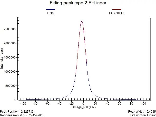
Crystal Quality Tester
-
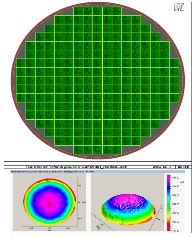
FRT Thickness Tester
×
![]()