1. Technical Overview
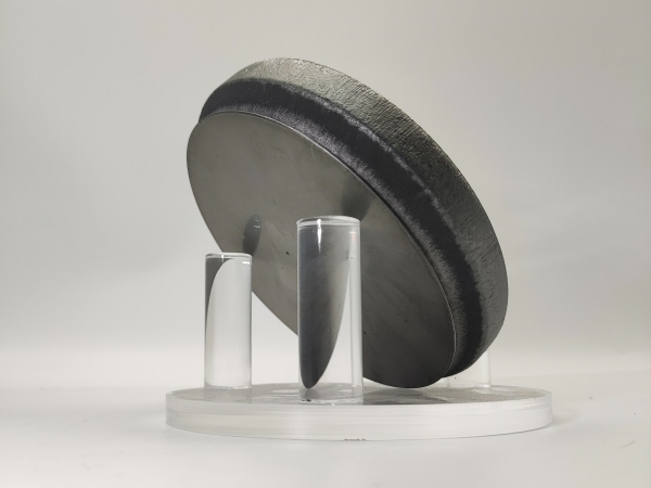
Diamond substrate wafers are categorized into three core types based on structural characteristics: single-crystal diamond substrates,
polycrystalline diamond substrates, and diamond thin films. These three categories differ significantly in grain structure, defect density, surface roughness, thermal stability, and interfacial adhesion, corresponding to distinct application scenarios in scientific research and industrial fields. The overall performance of diamond substrate wafers is fundamentally determined by the nucleation and fabrication process. The nucleation method directly affects grain uniformity, interfacial flatness, defect level, thermal stress stability, and service life of the final substrate products.
Currently, electrostatic seeding technology and Bias-Enhanced Nucleation (BEN) technology serve as the two mainstream fabrication processes in the industry. A series of differentiated techniques, including mechanical damage nucleation, adamantane chemical nucleation, and interlayer-assisted hybrid nucleation, have been developed to adapt to substrates of various materials, sizes, thicknesses, and precision requirements. This article systematically elaborates the technical principles, core advantages, limitations, and application boundaries of each process, providing reliable and practical guidance for process selection and customization in scientific research and industrial mass production.
2. Core Selection Logic for Diamond Substrate Fabrication
No universal nucleation process is applicable to all diamond substrate types. Single-crystal diamond substrates prioritize unified grain orientation, ultra-low defects, and grain-boundary-free structures; high-precision polycrystalline substrates focus on uniformity, stability, and mass producibility; industrial-grade substrates emphasize cost performance and universal adaptability; ultra-thin diamond films require extreme surface flatness and pinhole-free morphology. In actual R&D and production, process selection must be tailored according to substrate material, device application scenarios, precision indicators, and production scale, so as to avoid insufficient performance, low yield, and poor stability caused by process mismatch.
3. Detailed Analysis of Diamond Nucleation Processes
3.1 Mechanical Damage Nucleation: Low-Cost Solution for Industrial Polycrystalline Substrates
As one of the earliest industrialized diamond fabrication technologies, mechanical damage nucleation is mainly applied to low-cost and large-batch production of industrial-grade polycrystalline diamond products. The principle relies on physical treatments such as mechanical polishing, ultrasonic impact, and scratch processing to create micro-defects on the surface of silicon, sapphire, ceramic, and other substrates. Micro diamond debris is embedded to serve as natural nucleation sites, providing stable anchoring points for CVD diamond growth and facilitating the formation of continuous diamond layers. Featuring wide substrate compatibility and low equipment requirements, this process is widely adopted for industrial diamond protective coatings and general thermal dissipation substrates.

【Figure 1】SEM image of boron-doped diamond film grown on scratched silicon substrate
This process presents distinct physical characteristics under different operating modes. In mechanical polishing, smaller abrasive particles produce denser micro-defects and higher nucleation density, contributing to finer diamond grains. In ultrasonic-assisted nucleation, larger abrasive particles and lower dispersion medium density enhance particle impact kinetic energy, thereby improving nucleation efficiency. This method is compatible with insulating and semiconductor substrates and supports large-area batch fabrication.

【Figure 2】Relationship between abrasive particle size and nucleation density under polishing and ultrasonic treatment

【Figure 3】Influence of dispersion medium density on ultrasonic nucleation density
Nevertheless, this technology has obvious limitations. Physical processing parameters such as polishing intensity, ultrasonic duration, and abrasive ratio are difficult to standardize precisely, resulting in high surface roughness, poor batch-to-batch consistency, and elevated defect density. It is only suitable for industrial thermal management and wear-resistant protection scenarios and cannot meet the high-precision requirements of semiconductor devices, quantum devices, and advanced optical systems.
3.2 Adamantane Chemical Nucleation: Advanced Technology for High-Precision Ultra-Thin Diamond Films
To address the technical bottlenecks of ultra-thin diamond films and color-center customized diamond substrates in quantum technology research, adamantane chemical nucleation has emerged as a cutting-edge precision fabrication method. Traditional physical seeding struggles to achieve molecular-level uniform nucleation, easily causing pinholes, uneven thickness, and local defects in ultra-thin films. In contrast, adamantane molecules possess the same cage lattice structure as natural diamond with a molecular size of merely 1 nm, enabling ultra-uniform in-situ nucleation and fundamentally eliminating intrinsic defects in ultra-thin diamond films.

【Figure 4】Lattice structure comparison of adamantane, diamantane, and diamond cage units
Pure adamantane suffers from a low sublimation temperature of 250 °C, which cannot withstand the high-temperature CVD growth environment and leads to severe molecular loss and nucleation failure. To solve this problem, 2,2-divinyladamantane (DVA) functionalized molecules are adopted for substrate covalent immobilization, which effectively prevents high-temperature sublimation. Combined with precise low-temperature incubation regulation, the nucleation density can reach 6×10¹¹ cm⁻², enabling the preparation of pinhole-free, ultra-flat, and highly uniform ultra-thin diamond films.

【Figure 5】Molecular structure of DVA and schematic diagram of covalent bonding on silicon substrate

【Figure 6】Morphology evolution of diamond films with different low-temperature incubation durations
This process delivers exceptional nucleation uniformity, ultra-high surface flatness, and precise molecular doping controllability, making it ideal for quantum devices, high-precision optical films, and micro-sensor research. However, it involves complex synthesis and modification procedures, high production costs, and limited large-area uniformity, restricting its application to high-end scientific research and small-batch customized fabrication rather than large-scale industrial production.
3.3 Interlayer-Driven Hybrid Process: Customized Solution for Special and Irregular Substrates
For difficult-to-nucleate substrates with special materials or irregular structures, conventional seeding methods exhibit low nucleation efficiency and weak film adhesion. The interlayer-driven nucleation process introduces intermediate layers such as DLC amorphous carbon or metal carbide to construct a stable interfacial growth system. The intermediate layer precisely regulates carbon radical diffusion, suppresses substrate carbon loss and interfacial oxidation at high temperature, and induces uniform and stable diamond nucleation.
Furthermore, hybrid strategies combining ultrasonic pretreatment, low-temperature modification, and potential regulation can further optimize interfacial conditions, improving nucleation uniformity and film adhesion. This technique is highly compatible with customized irregular substrates and special functional substrates. Nevertheless, it suffers from relatively low nucleation density and inferior long-term film stability compared with mainstream electrostatic seeding and BEN processes, limiting its application to niche customized scenarios.
4. Horizontal Comparison of All Diamond Nucleation Technologies
To support accurate process selection, this chapter summarizes the core advantages, limitations, applicable substrate types, and typical application scenarios of the five mainstream diamond nucleation technologies, covering the full spectrum from industrial mass production to advanced scientific research.
| Nucleation Process |
Core Advantages |
Main Limitations |
Applicable Diamond Substrate Types |
Typical Application Scenarios |
| Electrostatic Seeding |
Wide substrate compatibility, excellent uniformity, mass producible, controllable defects |
Colloid agglomeration risk, incapable of oriented single-crystal growth |
High-precision polycrystalline substrates, ultra-thin diamond films |
Semiconductor thermal management, optical windows, precision electronic devices |
| BEN Bias-Enhanced Nucleation |
In-situ impurity-free growth, unified grain orientation, grain-boundary-free, ultra-low defects |
Only applicable to conductive substrates, narrow process window |
High-end single-crystal diamond substrates |
RF devices, quantum devices, superconducting devices, high-precision optical lenses |
| Mechanical Damage Nucleation |
Low cost, full substrate adaptability, low mass-production threshold |
High surface roughness, poor batch consistency, high defect density |
Industrial polycrystalline substrates, protective diamond films |
General equipment heat dissipation, wear-resistant industrial coatings |
| Adamantane Chemical Nucleation |
Molecular-level uniform nucleation, ultra-flat surface, precise doping capability |
Complex process, difficult for large-area mass production |
Ultra-thin diamond films, customized color-center substrates |
Advanced scientific research, quantum devices, ultra-high-precision optics |
| Interlayer-Driven Hybrid Process |
Adaptable to difficult-to-nucleate and irregular substrates, strong compatibility |
Relatively low nucleation density, ordinary long-term stability |
Special customized diamond film substrates |
Niche customized devices, irregular structural diamond functional layers |
5. Process Selection Summary
Each diamond nucleation process possesses unique advantages and application boundaries, and no single solution can cover all scenarios. For practical R&D and manufacturing, process selection should be determined by substrate size, thickness, precision requirements, base material, and terminal applications. High-end single-crystal precision devices prioritize BEN technology; semiconductor and optical polycrystalline products adopt electrostatic seeding; industrial thermal dissipation and wear-resistant scenarios apply mechanical nucleation; quantum research and ultra-precision thin films utilize adamantane chemical nucleation; irregular and special substrates adopt interlayer hybrid processes.
JXT provides a full range of high-quality diamond materials, including
high-consistency single-crystal diamond substrates, high-stability polycrystalline diamond substrates, and customized diamond films. We support sample research, small-batch customization, and large-scale mass production, fully meeting the R&D and manufacturing demands of the global diamond substrate industry.